Cookie Preferences

September 30, 2024

In an exciting development for the semiconductor industry, Adeia Inc. has announced its participation in several prestigious technology conferences. This move underscores Adeia's commitment to advancing hybrid bonding technology, a groundbreaking innovation set to revolutionize high-performance computing and AI applications.
Hybrid bonding has been generating significant buzz in the tech world, and for good reason. This cutting-edge technology promises to reshape the landscape of semiconductor design and manufacturing. As the demand for more powerful and efficient computing solutions continues to grow, Adeia's expertise in hybrid bonding positions the company at the forefront of this technological revolution.
Over the coming months, Adeia's top experts will be sharing their knowledge and insights at three major industry events. Each presentation will offer a unique perspective on hybrid bonding technology, highlighting its potential to transform various aspects of semiconductor production.
The conference tour kicks off at the IMAPS Conference in Boston, running from October 1-3, 2024. Here, Dr. Guilian Gao, a distinguished engineer from Adeia, will deliver an invited presentation on "Hybrid Bonding Process Technology." Attendees can look forward to a comprehensive overview of market demands driving the adoption of hybrid bonding, along with technical insights into the process and projections for future developments.
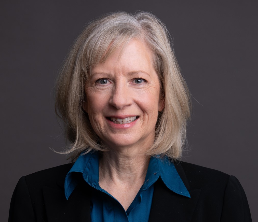
Following this, the spotlight shifts to Europe for the International Conference on Planarization/CMP Technology (ICPT) in Wiesbaden, Germany, from October 16-18, 2024. Dr. Laura Mirkarimi, Adeia's head and senior vice president of semiconductor engineering, will take the stage to discuss "CMP, A Key Enabling Process for Hybrid Bonding." Her talk promises to shed light on the critical role of chemical mechanical polishing in advancing hybrid bonding technology, offering valuable insights for industry professionals and researchers alike.
The final stop on this global tour of innovation will be the IEEE CPMT Symposium Japan (ICSJ) in Kyoto, from November 13-15, 2024. Here, Dr. Bongsub Lee, a director within Adeia's semiconductor engineering team, will present on "Hybrid Bonding in Advanced Heterogeneous Integration: Key Metrology Enablers." This presentation will delve into the innovative metrology techniques that are crucial for ensuring the quality and reliability of hybrid bonding processes.
These presentations are more than just technical discussions; they represent a window into the future of semiconductor technology. As Adeia continues to push the boundaries of what's possible with hybrid bonding, industry professionals, researchers, and tech enthusiasts alike will have the opportunity to glimpse the next generation of computing solutions.
The implications of Adeia's work extend far beyond the realm of semiconductors. By enabling more powerful and efficient computing technologies, hybrid bonding has the potential to accelerate advancements in artificial intelligence, data processing, and a wide range of applications that rely on high-performance computing.
For those eager to stay at the cutting edge of semiconductor technology, these conferences offer an unparalleled opportunity to learn from some of the brightest minds in the field. Adeia's presentations promise to provide valuable insights into the current state of hybrid bonding technology, as well as exciting projections for its future development and application.
As we look towards a future increasingly driven by advanced computing technologies, Adeia's work in hybrid bonding stands as a testament to the power of innovation. By sharing their expertise at these prestigious conferences, Adeia is not just showcasing their technological prowess; they're helping to shape the future of the entire semiconductor industry.
To learn more about Adeia and their groundbreaking work in hybrid bonding technology, visit their website at www.adeia.com. As the conference dates approach, tech enthusiasts and industry professionals alike will be eagerly anticipating the insights and innovations that Adeia is set to unveil.
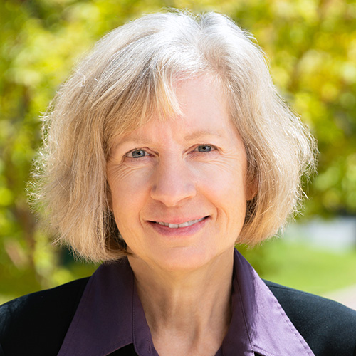
Laura Mirkarimi is SVP, Head of Semi Engineering at Adeia Semiconductor, San Jose, California. She earned a PhD in Materials Engineering at Northwestern University and a B.S. in Ceramic Sci. & Eng. from Pennsylvania State University. Dr. Mirkarimi leads the Engineering team at Adeia. Known for her pioneering work in hybrid bonding, she continues to focus on key technologies to enable future generations of electronic products including advanced packaging, metrology and thermal solutions. She holds over 100 patents and 60 technical publications. Prior to joining Adeia, she developed electronic devices including ferroelectric memory, transparent conductors and photonic crystal sensors at Hewlett Packard Laboratories for 12 years. As VP of Electronics Segment Marketing at Zeiss Microscopy, she worked with the R&D and product manufacturing teams to build the product roadmap for x-ray microscopy.
Laura Mirkarimi is SVP, Head of Semi Engineering at Adeia Semiconductor, San Jose, California. She earned a PhD in Materials Engineering at Northwestern University and a B.S. in Ceramic Sci. & Eng. from Pennsylvania State University. Dr. Mirkarimi leads the Engineering team at Adeia. Known for her pioneering work in hybrid bonding, she continues to focus on key technologies to enable future generations of electronic products including advanced packaging, metrology and thermal solutions. She holds over 100 patents and 60 technical publications. Prior to joining Adeia, she developed electronic devices including ferroelectric memory, transparent conductors and photonic crystal sensors at Hewlett Packard Laboratories for 12 years. As VP of Electronics Segment Marketing at Zeiss Microscopy, she worked with the R&D and product manufacturing teams to build the product roadmap for x-ray microscopy.
© 2026 Adeia Inc. All Rights Reserved |
Terms & Conditions |
Privacy Policy |
Accessibility