Cookie Preferences



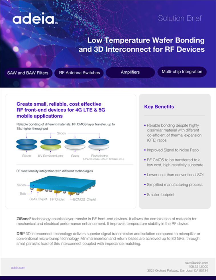
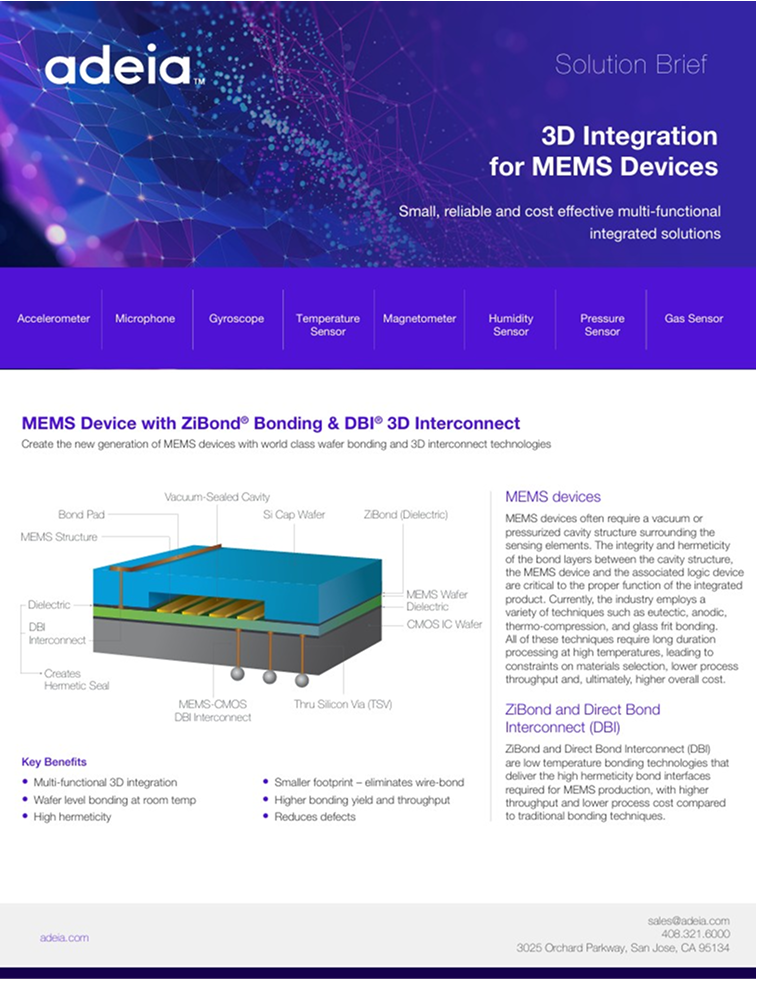
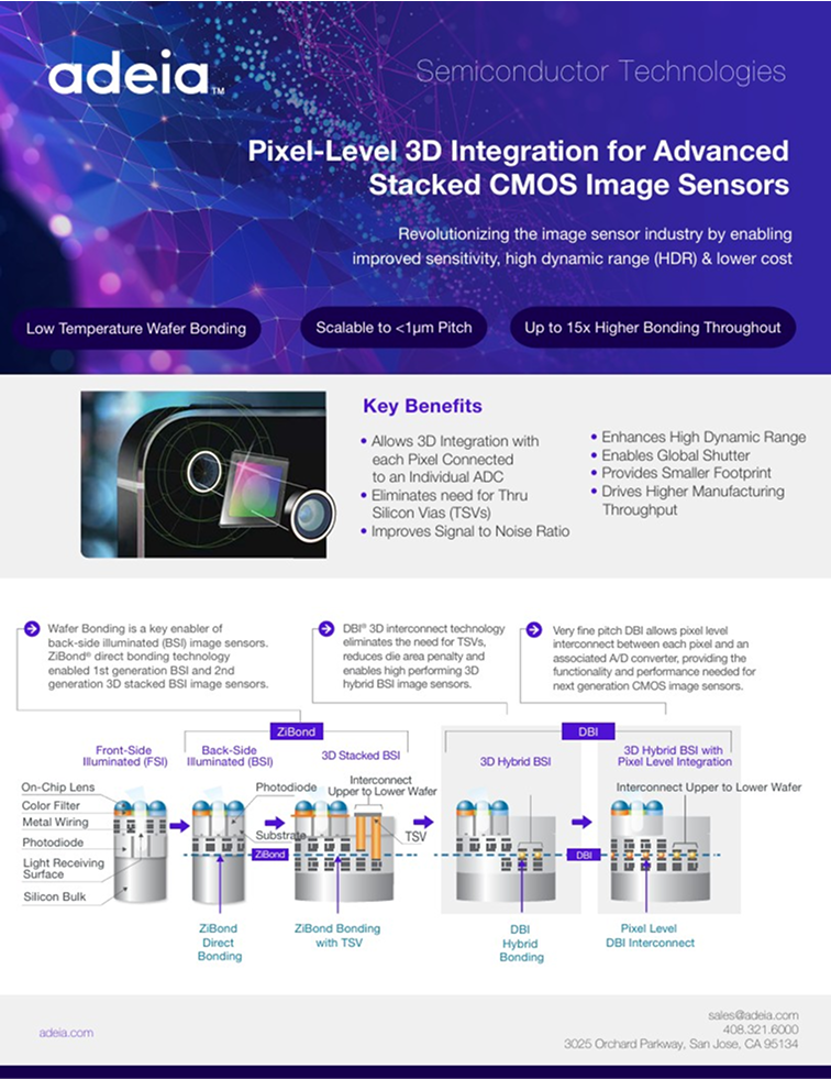
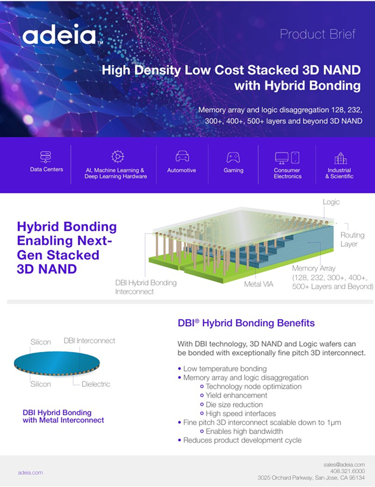
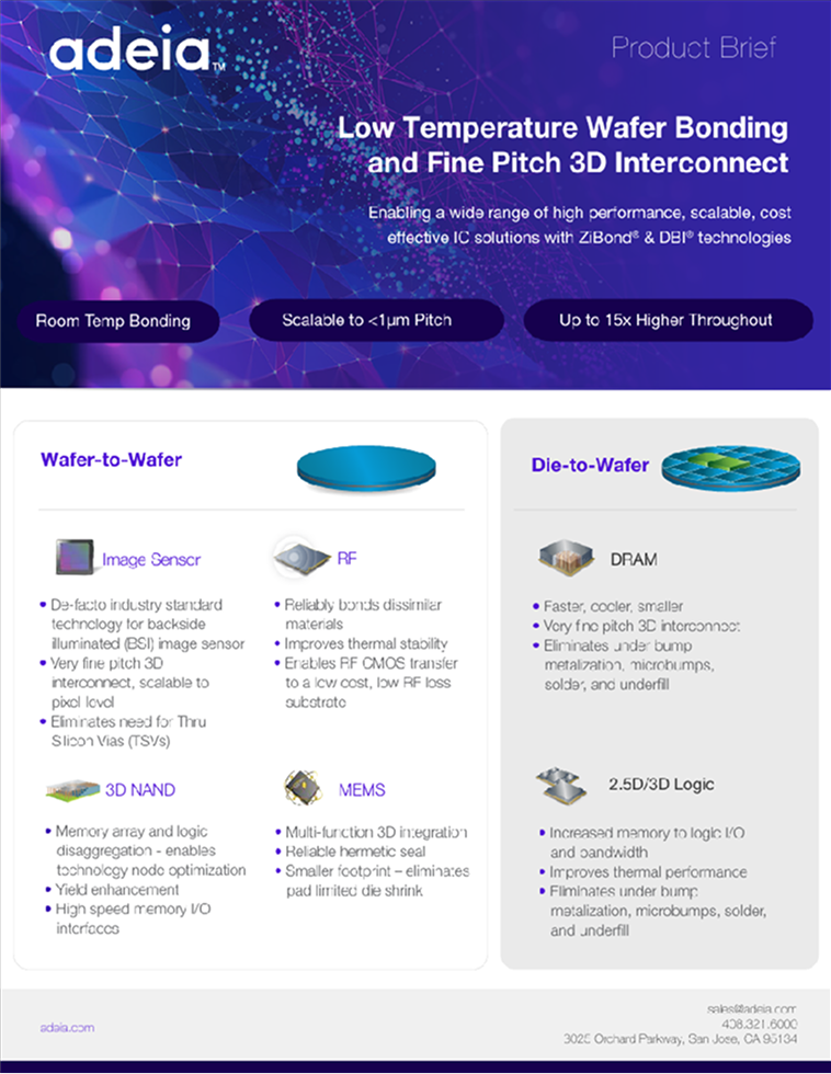
Our DBI wafer-to-wafer hybrid bonding platform creates strong bonds between both dielectric and metal surfaces to form a scalable electrical interconnect to ultra-fine, sub-micron pitches. It reduces the need for Through-Silicon Vias (TSVs) and eliminates the need for under-bump metal and underfill while boosting bonding throughput. This innovative approach also enhances electrical, thermal, and mechanical performance.
With existing production lines, DBI Wafer-to-Wafer hybrid bonding has proven to be cost-effective, versatile, and compatible with a range of industry standards in semiconductor wafer dielectrics, including silicon dioxide (SiO2) and silicon oxynitride-carbide (SiOxNyCz). It is even compatible with wafers that have different coefficients of thermal expansion (CTEs) like silicon (Si), aluminum oxide (Al2O3), glass, gallium arsenide (GaAs), and indium phosphide (InP) for heterogeneous integration.
%201.png)
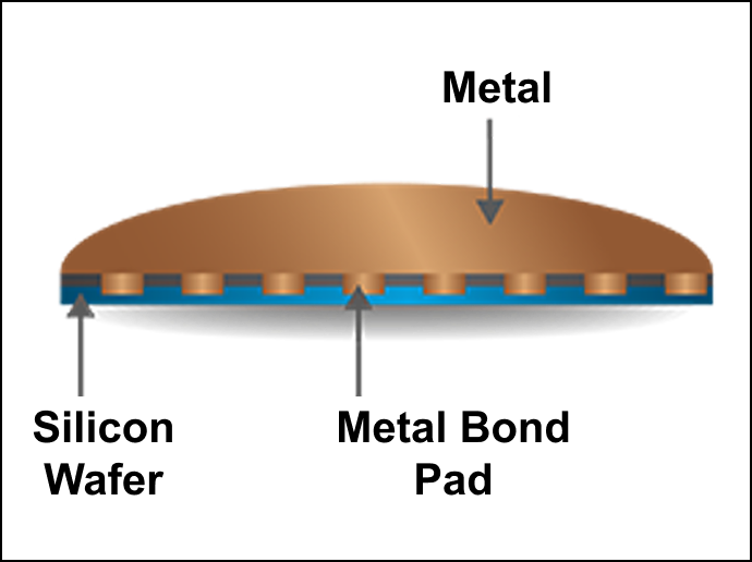
Metal bond pads are created with a BEOL process
%208.png)
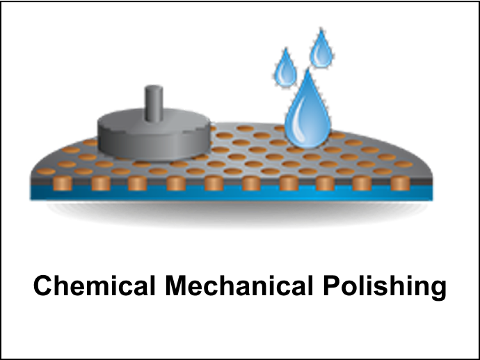
Wafer surface is planarized and polished to achieve smooth surfaces with a minimal Cu recess
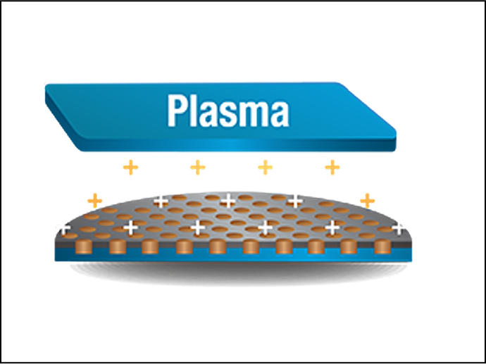
Plasma-based chemical activation prepares the surface for sopntaneous bonding
Plasma-based chemical activation prepares the surface for sopntaneous bonding
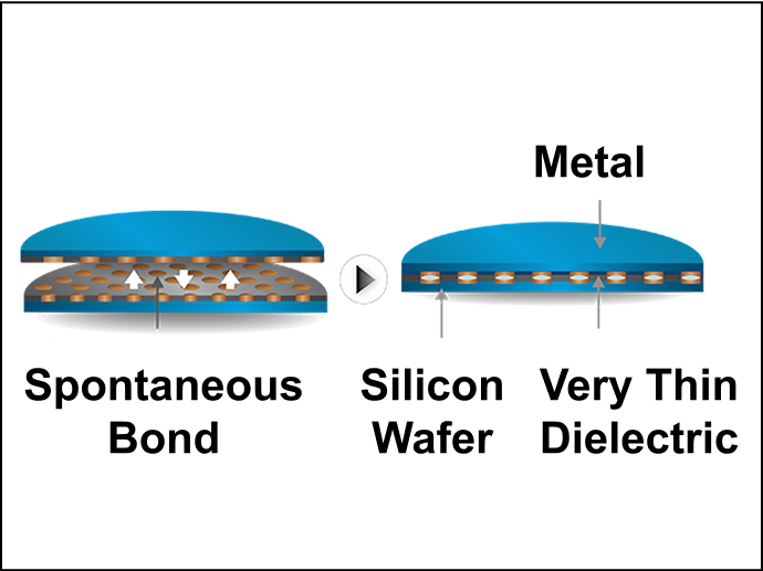
Prepared wafers are precisely aligned then placed together
Wafers sopntaneously bond at room temperature and pressure, forming strong chemical bonds in seconds
.png)
Plasma-based chemical activation prepares the surface for sopntaneous bonding
Through our Technology Transfer Program, we act as an extension of your R&D team to help you accelerate product development cycles utilizing our groundbreaking innovations.
Get in touch%20(1).png)
%20(2).png)
© 2026 Adeia Inc. All Rights Reserved |
Terms & Conditions |
Privacy Statement|
Accessibility
