
Cookie Preferences


According to analysts at Gartner, semiconductors designed to execute AI workloads will represent a $53.4 billion revenue opportunity for the semiconductor industry in 2023, an increase of 20.9% from 2022. AI-centric semiconductor revenue will continue to experience double-digit growth over the next few years, increasing 25.6% in 2024 to $67.1 billion and reaching $119.4 billion by 2027.
To understand the full ramifications of these market and technological forces on the industry and determine the role hybrid bonding technology will play in ensuring that chip processing power is in place to support AI use cases, we caught up with Dr. Seung Kang, who leads semiconductor strategic intellectual property (IP) and business development for Adeia.
Here is what he had to say:
Dr. Kang: It is dramatically impacting the industry because it is accelerating the need for increasingly powerful and energy-efficient computing systems, surpassing the capabilities of incumbent semiconductor platforms.
Let me elaborate.
AI workloads are computationally intensive, demanding semiconductor systems that are customized for massive parallel computing. Currently, the key drivers of such systems are a graphics processing unit (GPU) and high-bandwidth memory (HBM) which are coherently integrated with high-speed interconnects. To meet state-of-the-art AI system requirements, unprecedented performance benchmarks are needed. This is especially true when dealing with large language models. However, both processors and memory components face fundamental semiconductor scaling challenges.
GPUs and AI-customized neural processors rely on cutting-edge logic nodes that offer a smaller footprint, lower power consumption and faster speed. As the demand for computing performance continues to grow, realizing such processors on a monolithic chip — even at the most advanced node — becomes increasingly challenging. In such cases, the desired approach is to disaggregate and reassemble chips in new form factors without significant trade-offs.
Dr. Kang: Concerning memory, issues with DRAM bandwidth and capacity have existed for some time now. Since the industry first introduced HBM with four layers of vertically stacked DRAM, applications now require stacking of up to eight to twelve layers. Today, HBM applications face challenges in interconnecting more layers while simultaneously increasing throughput and improving thermal performance.
As a result, the success of next-generation AI semiconductor systems hinges on an advanced solution capable of interconnecting various dies without sacrificing the generic benefits of monolithic logic chips while also overcoming the limitations of incumbent HBMs.
There is a growing consensus in the industry that hybrid bonding technology will become widely adopted both for processors and for HBMs. Compared with other methods, hybrid bonding offers inherent advantages in high-density IO (input-output), reduced parasitic delay, shorter height and improved thermal performance.
Furthermore, it is a direct bonding process at low temperature which does not require extra materials and related process steps. In short, hybrid bonding can realize powerful multi-chip AI systems in a quasi-monolithic way.
Kang: Adeia has consistently been at the forefront of pioneering and enhancing hybrid bonding technology. In 2015, Adeia acquired intellectual property rights for hybrid bonding technology and has since maintained its commitment to organic research and development to advance this significant innovation in the semiconductor space.
Adeia not only licenses its comprehensive hybrid bonding portfolio to various semiconductor markets, including memory, logic, RF and image sensor, but also provides support to partners through technology transfers.
Hybrid bonding finds applications today in 3D heterogeneous integration scenarios where different types of chips – designed for different functions or from different suppliers – are seamlessly integrated and made interoperable.
The evolving requirements of AI systems are expected to surpass the capabilities of conventional semiconductor system architectures. This trend is driving the industry towards adopting disaggregated multi-chip configurations. Hybrid bonding is well-positioned as a compelling technology to underpin and facilitate these innovative semiconductor architectures.
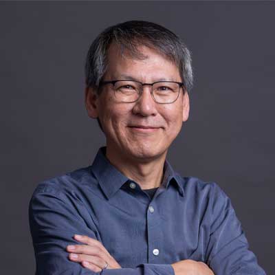
Dr. Seung Kang serves as Senior Vice President of Semiconductor Strategy and Pathfinding at Adeia, where he oversees strategic semiconductor programs encompassing technology, design, and system co- optimization. Prior to joining Adeia, Dr. Kang held a distinguished career at Qualcomm Technologies, Inc., where he spearheaded the Advanced Memory Program, pioneering early R&D and IP validation across the semiconductor ecosystem. His leadership also extended to the development of foundational logic IP for semiconductor nodes ranging from 7 nanometers down to 3 nanometers, supporting Qualcomm's flagship mobile, automotive, AI, and IoT products. Before his tenure at Qualcomm, Dr. Kang made significant contributions at Lucent Technologies Bell Laboratories and Lawrence Berkeley National Laboratory. He earned his B.S. and M.S. degrees from Seoul National University, Korea, and a Ph.D. from the University of California, Berkeley. Dr. Kang is a highly accomplished inventor, holding 250 U.S. patents and over 1000 patents granted globally. His research contributions are widely recognized, with over 100 published papers. He served as a Distinguished Lecturer for the IEEE Electron Device Society.
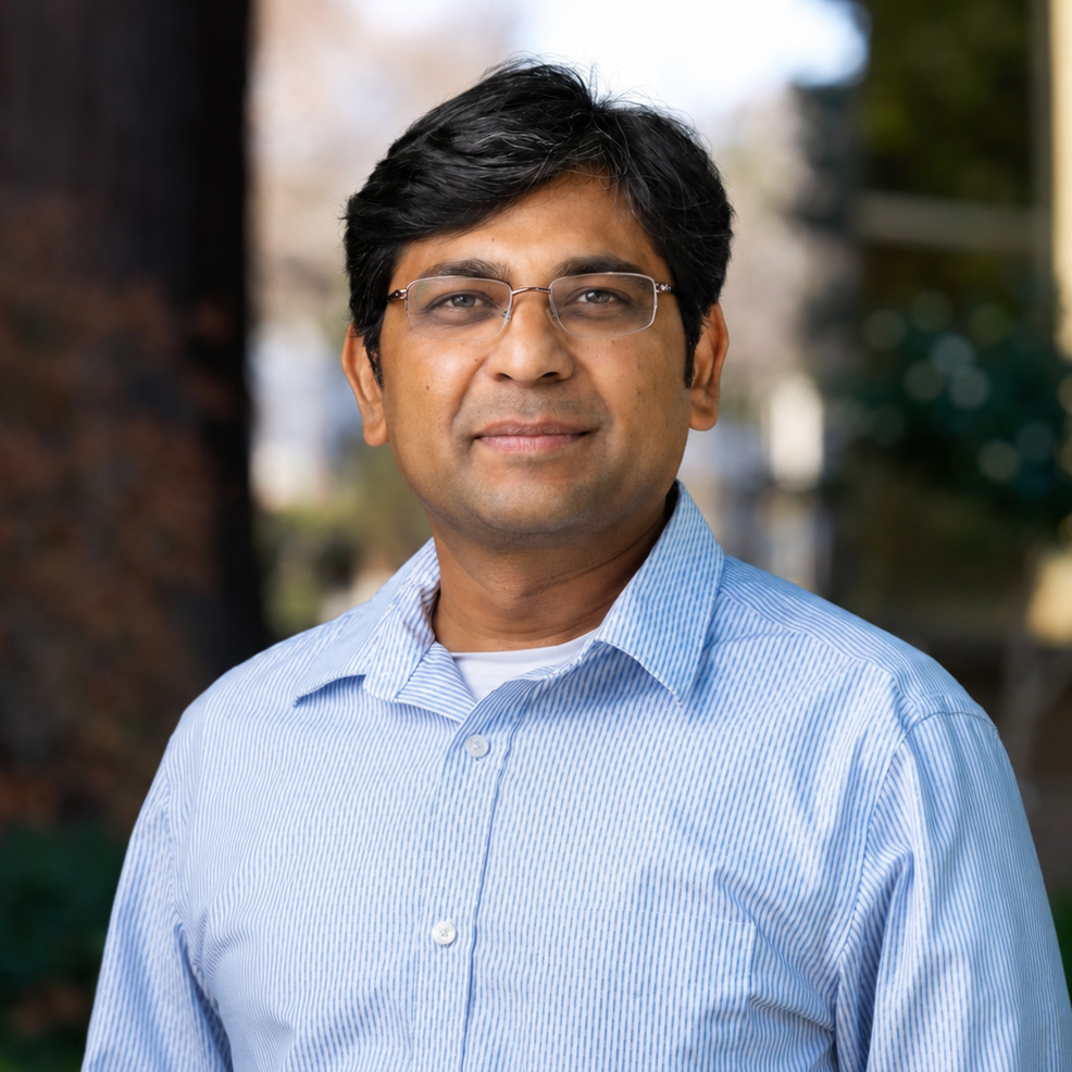
Rajesh serves as a VP of “Emerging Technologies, Semiconductors” at Adeia with a primary objective to identify and develop Adeia’s next semiconductor technology platform. In this role, Rajesh works closely with Adeia’s Chief Semiconductor Officer to identify and prioritize high-impact innovation areas and growth pathways across semiconductor markets and ecosystems and provide clear direction for R&D and IP development. Rajesh also leads Adeia’s Discovery, reliability and failure analysis labs.
Prior to this role, Rajesh led Adeia’s Patent Engineering organization and provided technical expertise in driving patenting activities including licensing, strategic prosecution, acquisitions, and assertion. Prior to this, Rajesh held several technical roles to advance Adeia’s internal R&D programs and spearhead innovation and idea generation activities at Adeia. Prior to joining Adeia over 18 years ago, he developed novel optical projection and illumination systems in a startup environment. Rajesh is a prolific inventor with over 200 US issues patents and more than 750 patents and applications worldwide.
He has authored more than 50 technical papers and presented in several international conferences. Rajesh has a Ph.D. in Engineering from Virginia Commonwealth University and a bachelor’s degree in Electrical Engineering from Visvesvaraya National Institute of Technology, Nagpur, India.
© 2026 Adeia Inc. All Rights Reserved |
Terms & Conditions |
Privacy Statement|
Accessibility