Cookie Preferences



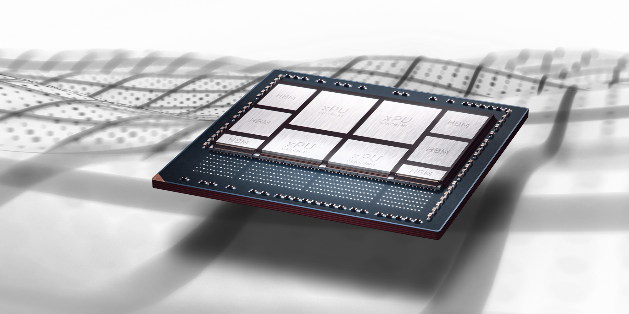

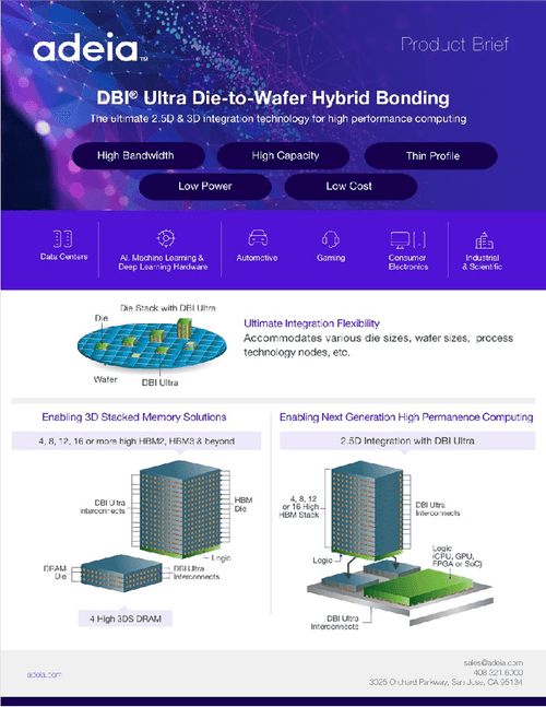
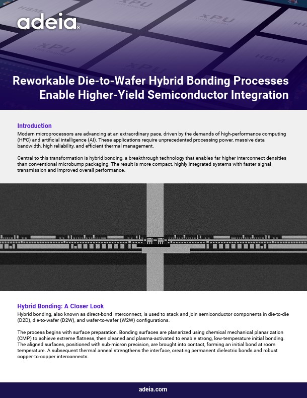
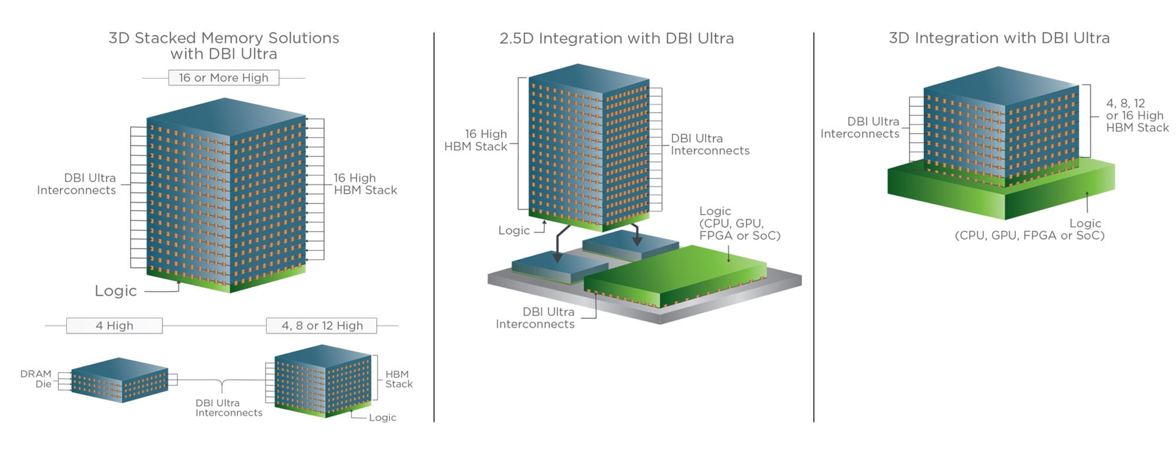
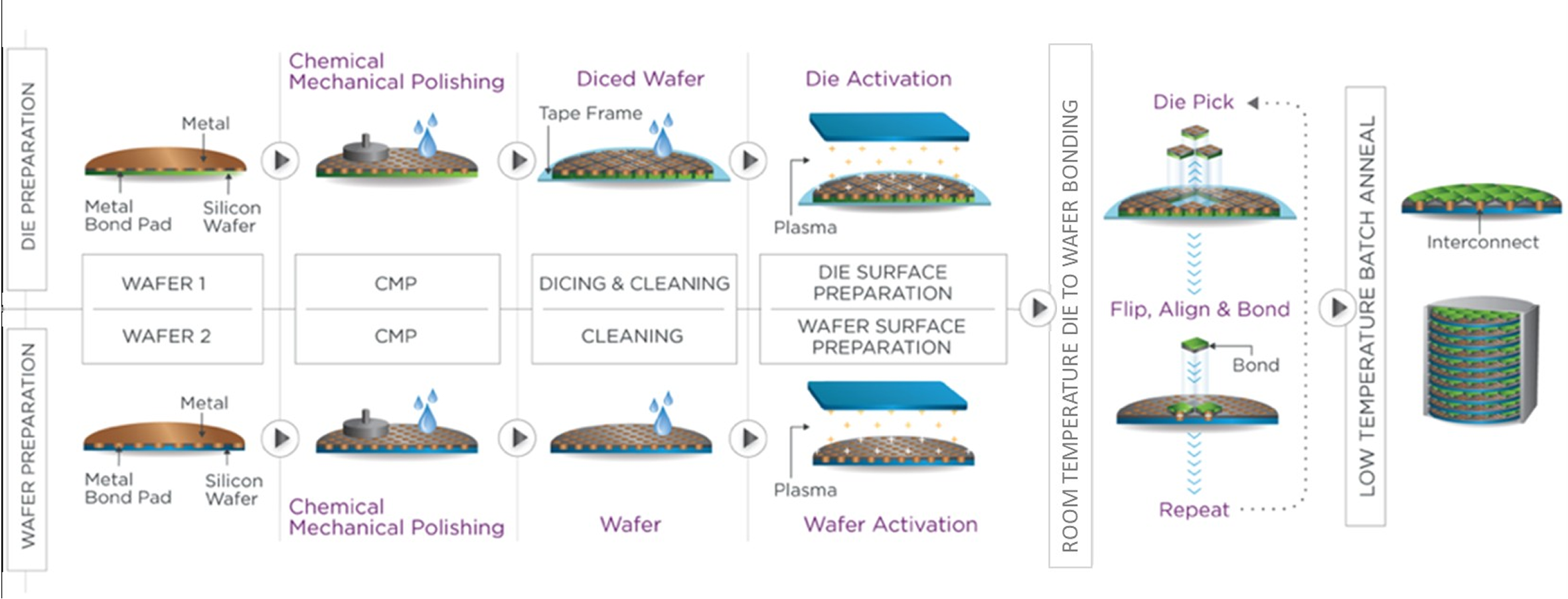
DBI Ultra is a cutting-edge, low-temperature hybrid bonding technology platform designed for die-to-wafer and die-to-die stacking. It enables seamless integration of dies of any size, across diverse technology nodes, wafer sizes, and materials, delivering unmatched flexibility for advanced semiconductor designs. Optimized for heterogeneous integration, DBI Ultra supports 2.5D, 3D, and 3.5D architectures, making it ideal for high-performance compute products including HBM, CPUs, GPUs, and TPUs. By eliminating traditional interconnect limitations, DBI Ultra enhances performance, power efficiency, and density, shaping the future of semiconductor innovation.
%202.png)
%208.png)
%2010.png)
%2011.png)
%202.png)
Through our Technology Transfer Program, we act as an extension of your R&D team to help you accelerate product development cycles utilizing our groundbreaking innovations.
Get in touch%20(1).png)
%20(2).png)
© 2026 Adeia Inc. All Rights Reserved |
Terms & Conditions |
Privacy Statement|
Accessibility
