Cookie Preferences


Adeia recently joined Roth Capital Partners for a Tech Talk exploring two breakthrough technologies shaping the next decade of semiconductors: hybrid bonding and direct-to-chip cooling.
Hosted by Scott Searle, Roth Capital’s Communications, AIoT,and Edge AI Analyst, the session featured Dr. Laura Mirkarimi, SVP Headof Engineering at Adeia, and Chris Chaney, VP of Investor Relations.
Together, they discussed how Adeia’s foundational technology development and innovative intellectual property are helping to solve some ofthe most critical challenges in AI, data center, and high-performance computing design — from interconnect scaling to heat management.
For those who missed the live discussion, here’s a recap of the keyinsights, industry context, and what lies ahead for Adeia’s hybrid bonding andour RapidCool™ technology.
The conversation began with a reality the industry knows well: monolithicsystem-on-chip (SoC) design is reaching its limits. As chips grow larger to support AI workloads, yields drop and costs soar. Integrating diverse functions — logic, SRAM, and I/O — on a single die forces process compromises and bottlenecks, particularly as SRAM scaling slows. The solution? Disaggregation of distinct functions into a chiplet architectures.
Implementing different functions on separate die makes it possible to optimize each functional unit, not just from a design perspective but also from a manufacturing process perspective. These separate dies are then connected within a single package, enabling higher yield, mixed process nodes, and faster time-to-market. But to fully realize chiplets’ potential, the interconnect between those dies must deliver monolithic-like performance. That’s where hybrid bonding enters the picture.
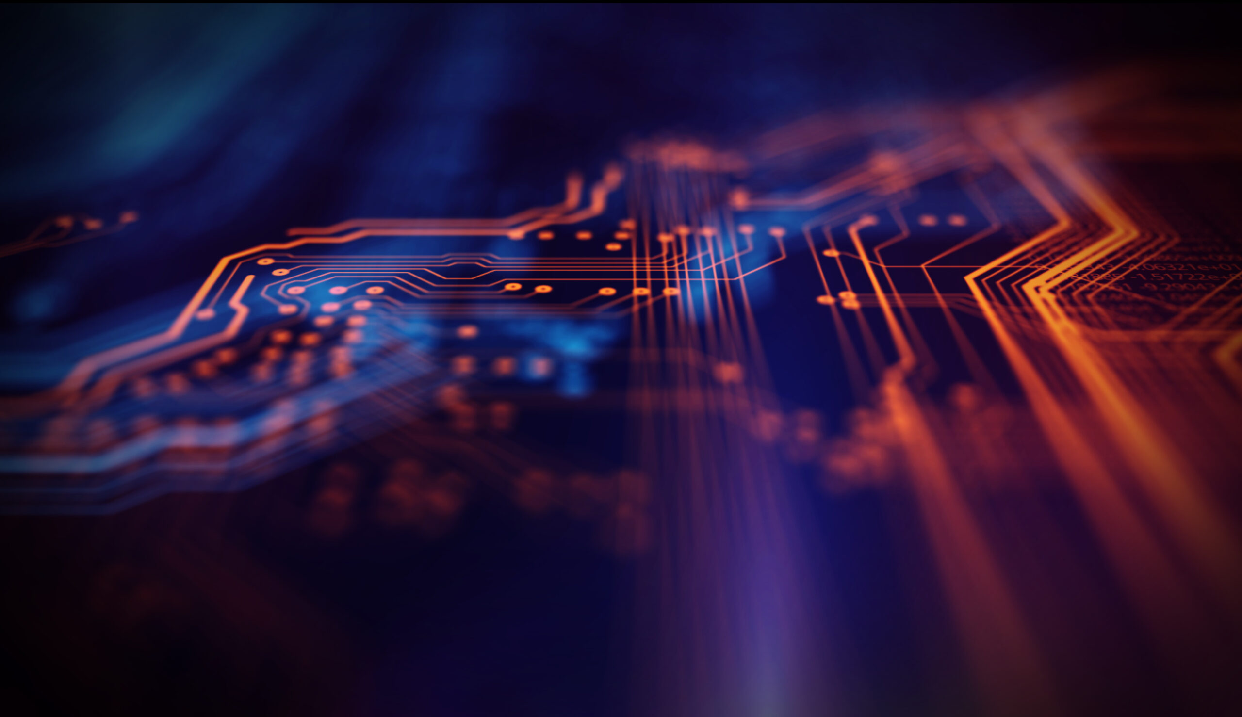
Hybrid bonding is the technology that allows dies to be bonded directly — oxide-to-oxide and copper-to-copper — without solder bumps or underfill. The result is a connection with no standoff, minimal parasitics, and pitches down to the micron scale, enabling massive bandwidth and power efficiency in 3D integrated designs compared to other bonding approaches.
As Dr. Mirkarimi explained, hybrid bonding “makes chips behave as if they were monolithically fabricated,” but with the flexibility and scalability that next-generation architectures demand.
Traditional microbump interconnects are comfortable around 35µm pitch — sufficient for low I/O count applications, but inadequate for dense memory or logic stacks.
Adeia and its partners have already demonstrated ~4 µm pitch indie-to-wafer configurations while high volume manufacturing is at a 9 µm pitch (as used by AMD), with research showing sub-micron wafer-to-wafer bonding feasible.
Modern die-to-wafer bonding equipment now achieves ±100 nm alignment (3σ), paving the way for 1 µm and below interconnects —and a roadmap that extends more than a decade into the future.
As Mirkarimi noted, “The physics of copper hybrid bonding does not impose a fundamental limit; it’s really about yield and backend process control.”
In 3D NAND, hybrid bonding connects logic and memory at around 1 µm wafer-to-wafer pitch. Adeia licensees such as Kioxia and Western Digital have already announced products using the technology, with further adoption expected across memory makers by 2026.
As data-center AI accelerators move to 16-high HBM and higher stacks, thermal management becomes a bottleneck. Hybrid bonding reduces junction-to-junction temperature differentials, keeping memory operating at higher frequencies with greater reliability.
Industry consensus now points to HBM4E (2026-2027) as the key inflection point for hybrid-bonded DRAM.
For logic, hybrid bonding enables SRAM-on-logic stacking and chiplet-to-chiplet integration with monolithic-like performance. AMD, Broadcom, NVIDIA, and major hyperscalers are all developing around this architecture — many through TSMC’s 3DFabric™ ecosystem, where Adeia’s IP plays a critical role.
Adeia researchers invented many foundational elements of hybrid bonding technology, and the company holds key patents for hybrid bonding and related science. Adeia continues to be the technology pioneer and IP leader in hybrid bonding that offers technology transfer to their customers who want an accelerated path to manufacturing.
The company’s portfolio — now over 1,100 active patent assets in bonding — spans materials, processes, chemistries, integrated circuit structures and system architectures, providing the foundational building blocks for the industry’s hybrid bonding ecosystem.
This includes:
Beyond patents, Adeia’s early partnerships with equipment suppliers like BESI and Lam Research ensure that the supply chain and process control required for mass adoption are in place.
As Mirkarimi put it, “We think holistically — from defect mechanisms to copper grain structure — so the industry can manufacture at scale with confidence.”
Once the technology is proven sound in our laboratory, we work directly with our customers to enable their supply chain with our Technology Transfer Program. Here we use a copy exact approach that teaches the process details, metrology specifications and the fundamental physics of the hybrid bonding technology.
If hybrid bonding addresses interconnect density, Adeia’s RapidCool™ technology tackles the next great challenge: thermal density.
AI and high-performance chips are exceeding 0.6W/mm2 already and soon to reach 1.5 W/mm² power density. Conventional cold plates with thermal interface materials (TIMs) are reaching their limits.
Adeia anticipates the first commercial implementations within 3–5 years, with early evaluations already underway with strategic partners inthe AI data-center market.
Hybrid bonding and direct-to-chip cooling are complementary innovations.
As Mirkarimi explained, “When we give designers the ability to stack higher, they will — so we also need to help them cool it efficiently.”
Adeia’s strategy recognizes that performance, power, and thermal challenges are now deeply intertwined — and that solving them requires co-design across interconnect and cooling domains.
Watch the replay: Technology Talk with Roth Capital — “Hybrid Bonding and Direct-to-Chip Cooling” featuring Dr. Laura Mirkarimi and Chris Chaney"

Laura Mirkarimi is SVP, Head of Semi Engineering at Adeia Semiconductor, San Jose, California. She earned a PhD in Materials Engineering at Northwestern University and a B.S. in Ceramic Sci. & Eng. from Pennsylvania State University. Dr. Mirkarimi leads the Engineering team at Adeia. Known for her pioneering work in hybrid bonding, she continues to focus on key technologies to enable future generations of electronic products including advanced packaging, metrology and thermal solutions. She holds over 100 patents and 60 technical publications. Prior to joining Adeia, she developed electronic devices including ferroelectric memory, transparent conductors and photonic crystal sensors at Hewlett Packard Laboratories for 12 years. As VP of Electronics Segment Marketing at Zeiss Microscopy, she worked with the R&D and product manufacturing teams to build the product roadmap for x-ray microscopy.

Dr. Laura Mirkarimi is SVP, Head of Semi Engineering at Adeia Semiconductor, San Jose, California. She earned a PhD in Materials Engineering at Northwestern University and a B.S. in Ceramic Sci. & Eng. from Pennsylvania State University. Dr. Mirkarimi leads the Engineering team at Adeia. Known for her pioneering work in hybrid bonding, she continues to focus on key technologies to enable future generations of electronic products including advanced packaging, metrology, and thermal solutions. She holds over 100 patents and 60 technical publications. Prior to joining Adeia, she developed electronic devices including ferroelectric memory, transparent conductors, and photonic crystal sensors at Hewlett Packard Laboratories for 12 years. As VP of Electronics Segment Marketing at Zeiss Microscopy, she worked with the R&D and product manufacturing teams to build the product roadmap for x-ray microscopy.
© 2026 Adeia Inc. All Rights Reserved |
Terms & Conditions |
Privacy Statement|
Accessibility