Cookie Preferences


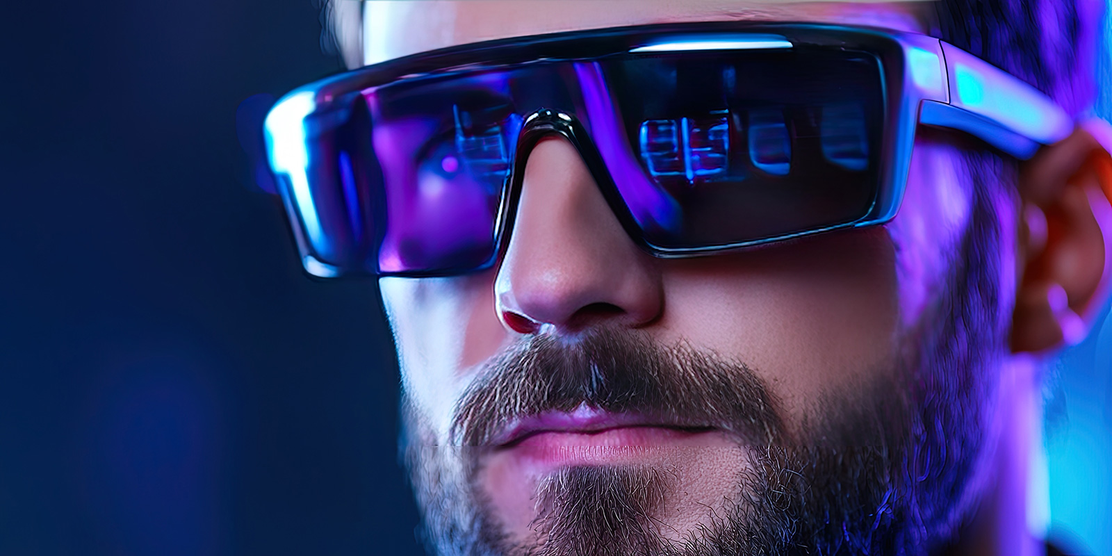
MicroLED technology is emerging as a pivotal innovation for augmented reality (AR) smart glasses, offering the potential for brighter displays, improved energy efficiency, and enhanced visual experiences. However, the path to widespread adoption is hindered by challenges in manufacturability and cost, primarily due to an underdeveloped supply chain. To overcome these obstacles, industry leaders are exploring advanced fabrication techniques and integration strategies that leverage existing semiconductor manufacturing ecosystems.
AR smart glasses require displays that are not only compact but also capable of high brightness and resolution to function effectively in various lighting conditions. MicroLEDs, with their self-emissive properties, high luminance, and potential for miniaturization, are well-suited for this application. Despite these advantages, the transition from prototype to mass production has been slow. The primary hurdles include the difficulty of producing ultra-fine gallium nitride (GaN) pixels smaller than 10 micrometers and integrating them with miniaturized silicon-based backplane circuits. These challenges are further exacerbated by the need for heterogeneous integration within the compact confines of wearable devices.
To address these challenges, researchers at Adeia are pursuing two key strategies:
By aligning MicroLED fabrication with established semiconductor processes, manufacturers can capitalize on the existing 300 mm high-volume silicon manufacturing ecosystem. This alignment facilitates the adoption of high-performance, low-power complementary metal-oxide-semiconductor (CMOS) backplane designs, which are essential for the functionality of AR displays.
The convergence of these strategies aims to establish a scalable and cost-effective production pathway for MicroLEDs in AR smart glasses. By leveraging the mature silicon manufacturing infrastructure and adopting advanced integration techniques, the industry can accelerate the commercialization of MicroLED displays. This progress is essential for meeting the growing demand for next-generation AR applications, where display performance and device affordability are critical to widespread adoption.
The future of AR smart glasses is closely tied to advancements in MicroLED technology. Adeia’s expertise in semiconductor integration and hybrid bonding is accelerating this shift, enabling high-performance, low-power MicroLED displays that help pave the way for affordable, next-generation AR solutions that transform user experiences.
Dr. Seung Kang serves as Senior Vice President of Semiconductor Strategy and Pathfinding at Adeia, where he oversees strategic semiconductor programs encompassing technology, design, and system co- optimization. Prior to joining Adeia, Dr. Kang held a distinguished career at Qualcomm Technologies, Inc., where he spearheaded the Advanced Memory Program, pioneering early R&D and IP validation across the semiconductor ecosystem. His leadership also extended to the development of foundational logic IP for semiconductor nodes ranging from 7 nanometers down to 3 nanometers, supporting Qualcomm's flagship mobile, automotive, AI, and IoT products. Before his tenure at Qualcomm, Dr. Kang made significant contributions at Lucent Technologies Bell Laboratories and Lawrence Berkeley National Laboratory. He earned his B.S. and M.S. degrees from Seoul National University, Korea, and a Ph.D. from the University of California, Berkeley. Dr. Kang is a highly accomplished inventor, holding 250 U.S. patents and over 1000 patents granted globally. His research contributions are widely recognized, with over 100 published papers. He served as a Distinguished Lecturer for the IEEE Electron Device Society.
Rajesh serves as a VP of “Emerging Technologies, Semiconductors” at Adeia with a primary objective to identify and develop Adeia’s next semiconductor technology platform. In this role, Rajesh works closely with Adeia’s Chief Semiconductor Officer to identify and prioritize high-impact innovation areas and growth pathways across semiconductor markets and ecosystems and provide clear direction for R&D and IP development. Rajesh also leads Adeia’s Discovery, reliability and failure analysis labs.
Prior to this role, Rajesh led Adeia’s Patent Engineering organization and provided technical expertise in driving patenting activities including licensing, strategic prosecution, acquisitions, and assertion. Prior to this, Rajesh held several technical roles to advance Adeia’s internal R&D programs and spearhead innovation and idea generation activities at Adeia. Prior to joining Adeia over 18 years ago, he developed novel optical projection and illumination systems in a startup environment. Rajesh is a prolific inventor with over 200 US issues patents and more than 750 patents and applications worldwide.
He has authored more than 50 technical papers and presented in several international conferences. Rajesh has a Ph.D. in Engineering from Virginia Commonwealth University and a bachelor’s degree in Electrical Engineering from Visvesvaraya National Institute of Technology, Nagpur, India.
© 2026 Adeia Inc. All Rights Reserved |
Terms & Conditions |
Privacy Statement|
Accessibility