Cookie Preferences


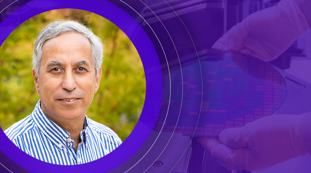
Bel Haba, a prolific inventor with over 600 US patents, recently sat down to discuss his remarkable career and the importance of mentorship in the semiconductor industry. Here are some key insights from our conversation:
A: After completing my studies at Stanford, I joined IBM's Yorktown Heights research center. It was there that I was surrounded by famous, accomplished people in small offices next to me. Their humility and achievements inspired me to pursue a similar path of innovation.
A: My first significant contribution was developing a method for machining slider heads for computers using pure water, eliminating the need for toxic materials. This work led to my first patent and opened doors to new opportunities.
A: Mentorship has been crucial. In the early years of my career, I made a point of "tagging along" with highly skilled individuals. I was continually impressed by how they thought outside the box and questioned everything. These experiences shaped my approach to problem-solving and innovation.
A: Look for a successful team and try to join them. Tag along with successful people - you'll learn not just technical skills, but also the art of innovation. Don't assume you know everything; be open to learning from those around you.
A: First, examine whether the problem can be solved with existing technologies. If it can, it probably will be. As a researcher, you should look beyond that - how can you solve it in a completely different way? Then, consider how your solution fits into the existing infrastructure. A great idea that requires a complete overhaul of current systems may struggle to be adopted.
A: Always ensure your solution doesn't break the laws of physics - you could waste years otherwise. Also, consider cost. A solution that's 80-90% as good but costs half as much will often win in the market. Your solution needs to be competitive, with a worthy performance-to-cost ratio.
A: In large corporations, you often work on a small piece of a bigger puzzle. In startups, you see the whole picture and understand how critical each component is. This global perspective is invaluable - it helps you see what's missing and what needs to be done.
A: I'm particularly interested in solving thermal and power delivery challenges, as well as the potential for virtual displays and micro-LEDs. These areas present trillion-dollar questions that could revolutionize how we interact with technology.
A: Stay curious, don't be afraid of being questioned, and always be ready to say "I don't know, but I'll look into it." Innovation is about constant learning and pushing boundaries. And remember, it's not just about having great ideas - it's about making them work in the real world.

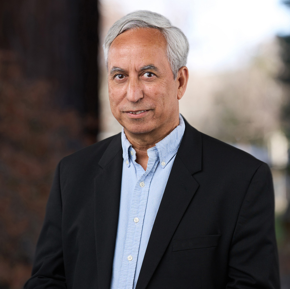
Laura Mirkarimi is SVP, Head of Semi Engineering at Adeia Semiconductor, San Jose, California. She earned a PhD in Materials Engineering at Northwestern University and a B.S. in Ceramic Sci. & Eng. from Pennsylvania State University. Dr. Mirkarimi leads the Engineering team at Adeia. Known for her pioneering work in hybrid bonding, she continues to focus on key technologies to enable future generations of electronic products including advanced packaging, metrology and thermal solutions. She holds over 100 patents and 60 technical publications. Prior to joining Adeia, she developed electronic devices including ferroelectric memory, transparent conductors and photonic crystal sensors at Hewlett Packard Laboratories for 12 years. As VP of Electronics Segment Marketing at Zeiss Microscopy, she worked with the R&D and product manufacturing teams to build the product roadmap for x-ray microscopy.
Dr. Belgacem Haba is Senior Technical Fellow and vice president at Adeia Semiconductor, San Jose, California. Prior to joining Adeia, he worked at IBM, Google, NEC, Rambus as well as Tessera/Xperi. He also co-founded SiliconPipe a start-up acquired by Samsung. Dr. Haba earned a Ph.D. and an M.S. in materials science materials science and engineering, and an M.S. in applied physics from Stanford University, California. He received a B.S. in physics from the University of Bab-Ezzouar, Algeria. Dr. Haba holds 660 granted U.S. patents and has authored numerous technical publications. His activities focus in developing next generations of electronics products and his research is in the advanced packaging of microelectronics including technologies such as hybrid and photonics interconnects and future thermal solutions.
© 2026 Adeia Inc. All Rights Reserved |
Terms & Conditions |
Privacy Statement|
Accessibility